A glimpse inside the nanoworld
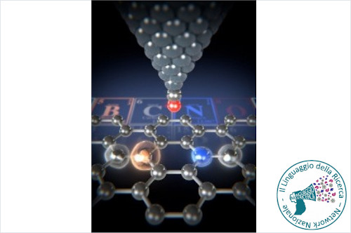
“There is plenty of room at the bottom”, Richard Feynman quotes and uses as title in one of his famous lectures1. Feynman smarty referred to the concept we all seem to listen nowadays, that is “nanotechnology”. This new scientific field has made possible to access a great number of applications using the lightest, smallest, nano-materials. But what is nanotechnology? What are the so-called nanomaterials and why are we interested in them? How can we study this tiny, yet extraordinary world that could fit on the tip of our finger? It was vital to develop the right tools in order to be able to actually see and observe these materials. The development of these microscopes initiated at 1980s making it possible for scientists to finally dive into researching and understanding these materials. In particular Atomic Force Microscopy (AFM), had a great impact on studying the morphology of several nano objects, understanding their characteristics, and correlating these with their properties. Another more specialized type of microscopy based on the same concept as AFM, Kelvin probe force microscopy (KPFM) can give us insight on the electronic properties of these under study materials, thus we can realize their potentials and apply them in future electronic applications, such as cameras of smartphones, batteries, and computer memory devices.
Vasiliki Benekou, CNR-ISOF-BO, Bologna
Documentazione
Bibliogafia
- Feynman, Richard P. (1960) - There's Plenty of Room at the Bottom